When you purchase through links on our site, we may earn an affiliate commission.Heres how it works.
Existing methods require bonding these materials onto silicon, a process thats both costly and wasteful.
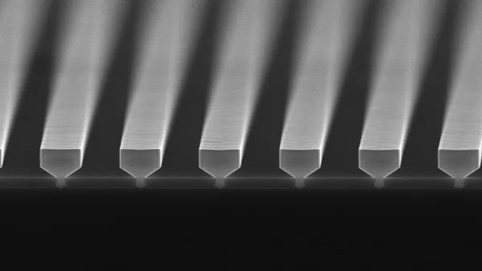
Gallium arsenide is then deposited into these trenches, where it only makes contact with silicon at the bottom.
A 300 mm silicon wafer containing thousands of GaAs devices with a close-up of multiple dies and a scanning electron micrograph of a GaAs nano-ridge array after epitaxy
This placement keeps any defects buried within the trench and prevents them from spreading into the laser material above.
